Stage 01
Design inputs
Circuit requirements, mechanical outline, connector positions, environmental conditions, expected build volume and cost expectations.
T · [CLIENT TO PROVIDE] E · [CLIENT TO PROVIDE]
By the time routing begins, most of a board's electrical behaviour has already been decided.
Overview
By the time routing starts, most of a board's electrical behaviour has already been decided: the layer stack-up, where the reference planes sit, how power is distributed, and where the noisy and sensitive sections live relative to each other.
We treat those as engineering decisions with reasons attached. Placement follows the signal flow and the thermal map. Routing follows the constraints the circuit actually needs, not a uniform rule applied everywhere.
Manufacturability is designed in from the start — realistic clearances, sensible component choices, accessible test points and fabrication notes that a manufacturer can follow without guessing.
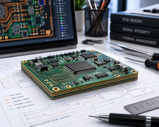
Board engineering
Each element below changes the electrical result. None of them is a formatting exercise.
Layer count, dielectric arrangement, reference plane placement and impedance targets defined before layout begins.
Readable, reviewable schematics with clear net naming, design intent captured and the review process built into the workflow.
Placement driven by signal flow, thermal distribution, mechanical constraints, connector positions and assembly practicality.
Constraint-driven routing with attention to critical nets, differential pairs, return paths and the loops that create emissions.
Reference continuity, decoupling strategy, supply impedance and terminations considered against the actual edge rates in the design.
Fabrication and assembly outputs, stack-up notes, test point access and documentation that reduces questions during the build.
Board process
A repeatable sequence with review gates where mistakes are still cheap to fix.
Stage 01
Circuit requirements, mechanical outline, connector positions, environmental conditions, expected build volume and cost expectations.
Stage 02
Layer arrangement, impedance targets, clearance rules and the routing constraints derived from the electrical requirements.
Stage 03
Schematics produced and reviewed as a team exercise, with errors caught on paper rather than on copper.
Stage 04
Component placement resolved against signal flow, thermal behaviour, assembly access and mechanical fit.
Stage 05
Critical nets first, then the remainder, with return paths and plane integrity maintained throughout.
Stage 06
Electrical rule checks, design rule checks, manufacturability review and a structured design review before release.
Stage 07
Complete data package released to the manufacturer with the notes and clarifications needed for a clean first build.
Consequences
| Decision | Why it matters | What we do |
|---|---|---|
| Layer stack-up | Sets impedance, return paths and noise coupling | Defined against the fastest signals and the power distribution need, before placement |
| Reference planes | A broken reference turns a good trace into an antenna | Plane continuity checked along every critical route, splits planned deliberately |
| Decoupling | Determines supply stability under switching load | Placement and value chosen for the actual current demand and frequency content |
| Thermal paths | Hot components shorten product life | Copper area, via arrays and placement zoning planned with the thermal map in mind |
| Test access | Undetectable faults cost more later | Test points and access planned with the production test strategy, not added afterwards |
Scope
Board types
Engineering focus
FAQ
What teams usually want to understand before handing over a board.
Either. We can lay out a board from your reviewed schematic, or take the circuit requirement and produce both schematic and layout. If we are laying out someone else's schematic, we review it first and raise anything that will cause trouble in copper.
That follows from signal speed, power distribution needs, component density and mechanical size. We set the stack-up as part of the design input stage and explain the reasoning rather than defaulting to a standard count.
Signal integrity is addressed as a design discipline throughout: stack-up, reference continuity, terminations and constraint-driven routing. The extent of formal simulation depends on the speeds involved and is agreed per project.
Yes. We prepare the manufacturing data package, respond to manufacturer queries and support first-article review. Manufacturing coordination scope is agreed per project.
Design source files, fabrication outputs, assembly drawings, bill of materials and documentation. Specific formats are agreed at the start so they fit your existing toolchain and manufacturer.
Share the circuit requirement, the mechanical outline and the environment. We will come back with the stack-up and the risks.